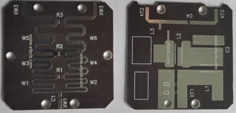
Key Features and Manufacturing Challenges of RF Microwave PCB
In today's interconnected world, wireless communication has become an integral part of our lives. From smartphones and smartwatches to Wi-Fi routers and satellite systems, the demand for high-performance wireless devices is constantly growing. At the heart of these devices lies a crucial component known as the RF Microwave PCB.
Manufacturing Challenges and Techniques
Manufacturing RF Microwave PCBs present unique challenges due to the tight tolerances and high-frequency requirements. Advanced manufacturing techniques are employed to meet these challenges:

- Precise Etching: RF PCBs require precise etching processes to create accurate trace widths and spacing. Techniques such as photolithography or laser direct imaging are used to achieve fine trace features and tight tolerances.
- Via Design: Proper placement and design are critical to maintaining controlled impedance and reducing signal loss. Blind vias, buried vias, and microvias are commonly used to interconnect different layers while maintaining signal integrity.
- Component Assembly: RF components, such as connectors, filters, and amplifiers, require careful soldering techniques to minimize signal loss and achieve consistent performance. Specialized soldering methods, such as reflow soldering or controlled temperature soldering, are employed to ensure reliable connections.
Key Features and Design Considerations:
- Material Selection: RF Microwave PCB are typically constructed using high-performance substrates such as PTFE (Polytetrafluoroethylene), ceramic-filled PTFE, or other high-frequency laminates. These materials offer low dielectric loss and excellent electrical properties necessary for minimizing signal distortion and maximizing signal integrity at high frequencies.
- Controlled Impedance: RF Microwave PCBs often require controlled impedance traces to ensure proper signal transmission. Impedance control is achieved through careful trace width, spacing, and dielectric thickness calculations. This helps in reducing signal reflections and maintaining signal integrity throughout the circuit.
- Grounding and Shielding: Proper grounding and shielding are crucial in RF Microwave PCBs to minimize interference and crosstalk between signal traces. Ground planes and shielding techniques, such as RF enclosures or metal shields, are employed to isolate sensitive RF components and prevent unwanted signal coupling.

RF Component Placement: The placement of RF
Microwave PCB is critical to achieving optimal performance. Careful
attention must be given to minimize signal path lengths, reduce transmission
line losses, and avoid unintended resonances. RF components should be
strategically placed to maintain signal integrity and minimize signal
degradation.
